SiC Technology for Industrial Power Electronics: Accelerating from Promise to Reality

Consumers and regulatory bodies alike are putting greater pressure on industry to minimize energy consumption — specifically for applications such as electrical motor systems and power supply units.
Electric motors are the single biggest consumer of electricity, accounting for an estimated 45% of global electricity consumption, according to a new analysis by the International Energy Agency. That is more than twice as much as lighting, the second-largest source of consumption.
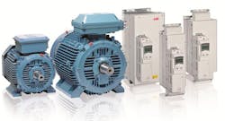
Variable speed drives (also called alternating current or AC drives) can reduce the energy consumption of motors by 50% in many applications, and yet less than 10% of motors are actually operated by drives. This represents a fantastic opportunity to bring about a dramatic reduction in electricity consumption by implementing new high performing AC drive technologies.
For decades, these industrial systems have run on conventional silicon-based diodes and transistors. Yet, ironically, their steadily increasing energy demands are pushing silicon-based semiconductor devices to their physical limits. The challenge facing industry is that it cannot reduce energy consumption without affecting productivity — unless it finds a way to consume energy more efficiently.
SiC to the Rescue
The search for a solution points naturally to next-generation wide-bandgap semiconductors, such as silicon carbide (SiC), that are better suited to efficiently handle the electrical loads, switching rates and other performance capabilities that industry requires to control energy consumption.
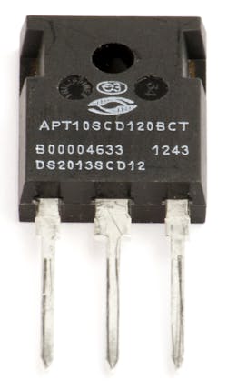
The variants and volumes of commercial SiC devices are rapidly multiplying. SiC diodes, in particular, have already appeared in photovoltaic inverters, power supplies for computer servers, uninterruptable power supplies and high-end AC drives for electrical motor systems.
Further upstream, recent advances in the manufacture of SiC wafers have accelerated the technology’s march to broader adoption. Specifically, the introduction of large-diameter (150-mm) SiC wafers with excellent crystal quality will increase manufacturing efficiencies and device yields per wafer. Both these factors will drive down device and system costs.
But what benefits are driving the adoption of SiC over incumbent silicon technology? Many stem from SiC’s unique combination of semiconductor properties such as its wide bandgap, excellent thermal conductivity, high electron mobility and high electrical breakdown field.
Electrons in SiC need about three times as much energy as they do in silicon to become excited enough to reach their conductive state. This factor, the material’s high electron mobility and its eight-fold higher electrical breakdown field allow SiC components to switch at higher frequencies, operate reliably at temperatures as high as 650 degrees Celsius and handle voltages up to 10 times higher.
In practical terms, SiC substrates’ ability to handle significantly higher voltages enables device fabrication with 10x thinner epitaxy structures. In addition to reducing footprint and complexity, thinner power electronic devices exhibit lower resistance, which helps to reduce losses and explain why SiC devices are much more energy efficient than those made from silicon.
Such SiC-based high-voltage power devices represent a major performance leap for new megawatt power systems.
Eliminating Roadblocks to SiC Adoption
Historically, the power electronics market has taken a wait-and-see approach to adopting SiC diodes and transistors. Most concerns have centered on questions about SiC’s cost, quality and reliability.
But these issues are quickly evaporating in the wake of recent technological advances.
• Cost: Current state-of-the-art SiC wafers measure 100 mm (4 inch) in diameter. While suppliers can maintain good crystal quality at this diameter, many existing power device fabs have moved to 150 mm (6 inch) and even up to 300 mm. The additional expenses to accommodate handling of smaller wafers in the manufacturing process flow drives up costs for devices. With the advent of 150-mm diameter SiC wafers, the per-wafer die count more than doubles, driving down overall costs while increasing manufacturing efficiency. Also, 150-mm SiC wafer production can be easily inserted in many mainstream silicon wafer fabs.

• Quality: Defects in the crystalline structure of semiconductor wafers contribute to device failures and lower yields. Controlling different types of defects has been a challenge and one of the major limitations of SiC wafer technology. Historically, the quality of each generation of new, larger wafers is lower compared to prior generations; however, SiC quality is gradually improving over time as suppliers scale and refine their manufacturing processes. The most common killer defect for devices made from SiC wafers is micropipes. As Dow Corning developed its crystal technology to achieve 150-mm crystals, it has maintained low micropipe densities at less than 1/cm2. The company was also able to maintain low levels of other defects, such as screw dislocations and basal plane dislocations in the expansion of SiC substrates to the 150-mm diameter.
The next step — scaling 150-mm wafer production to high-volume — is anticipated to occur over the next 12 to 18 months. Parallel improvements to SiC epitaxy — the deposition of SiC semiconductor layers with different doping concentration by a chemical vapor deposition process — have also been critical to this progress.
Yet even after production of 150-mm wafers ramps to high volume, other challenges will remain. One is the need for device packaging methods that can fully support SiC’s potential for high-temperature applications. Conventional semiconductor packaging materials are often limited to 175 degrees Celsius or lower — silicon’s typical operating threshold — and most hit a wall at 200 degrees Celsius. There are a number of companies working on this challenge, including Dow Corning, which is developing packaging solutions that perform reliably at 225 to 250 degrees Celsius.
One other concern is reliability of newly developed SiC transistor switches, which is critical for many industrial applications like variable speed drives used in electrical motor systems and power supplies. Designer are still optimizing gate oxide materials and deposition processes to ensure more reliable switching functions in promising new power electronic devices, such as SiC MOSFETs (metal oxide semiconductor field effect transistors). As a result, qualified SiC MOSFETs, JFETs (Junction FET) and BJTs (Bipolar Junction Transistor) products are increasingly available as more power semiconductor manufacturers refine their SiC device technology and commercialize discrete, hybrid and full SiC module solutions.
Benefits of SiC Devices for Industrial Power Electronics
Although today’s power devices are based on standard silicon technologies, analysts such as Yole Développement and IHS expect SiC to gradually replace them in a variety of power applications where high electricity consumption requires more efficient power electronics.
More specifically, SiC-based power electronics deliver an increased value in use compared to silicon in many industrial applications. This enabling technology enables engineers and system designers to benefit from:
• Significantly lower conduction and switching losses because SiC devices can be made much thinner. Such transistors and diode devices need to dissipate less waste heat because they operate much more efficiently than silicon.
• SiC devices supporting higher current densities compared to incumbent silicon device technology. This enables smaller die sizes and will allow SiC modules to have significantly smaller form factors, simpler assembly and lower materials costs.
• SiC electronics that can reliably operate at temperatures well exceeding 200 degrees Celsius. When appropriate packaging and interconnection technologies for these elevated operation temperatures become mainstream, the technology will then offer system designers more options to rethink thermal management of their products and reduce system costs.
• A significantly reduced temperature effect on operation due to wide bandgap properties of SiC which reduces the need to compensate for temperature drifts.
• Faster switching frequencies compared to silicon, shifting switching speeds of variable speed drives or power supplies beyond the audible frequency range (>15kHz) to reduce noise, minimize the size of electromagnetic interference filters and other passive components and enable more compact system sizes.
Conclusion
Analysts predict a steady rise in the adoption of SiC materials, devices and systems as this semiconductor technology matures, and as industrial applications call for both better performance and more energy-efficient systems.
Much work remains to be done to make SiC power electronics more viable; however, improvements in device design and performance, manufacturing yields and supply chain competition are helping to shift SiC technology into mainstream industrial applications. Costs will also fall further as 150-mm SiC wafers ramp up to volume production in standard fabs.
More importantly, SiC technology finally offers the industrial sector the means to reduce energy consumption without compromising on productivity.
Markus Behet is Global Market Manager for Dow Corning’s Power Electronic business. The business aims to develop and commercialize compound semiconductor solutions for industrial applications, such as AC drives, uninterruptable power supplies and power supplies based on power factor correction, as well as other emerging applications such as transportation and energy. Based in Germany, Markus is also responsible for the global strategic direction and commercialization of Dow Corning’s wide-bandgap semiconductor solutions, like gallium nitride-on-silicon and high-voltage silicon carbide epiwafer products.